Does the process work?
Establish the method, characterize variables, and qualify the process window.
Advanced optical packaging, from die-level process development in California to production transfer in Thailand—with experience on both sides of the handover.
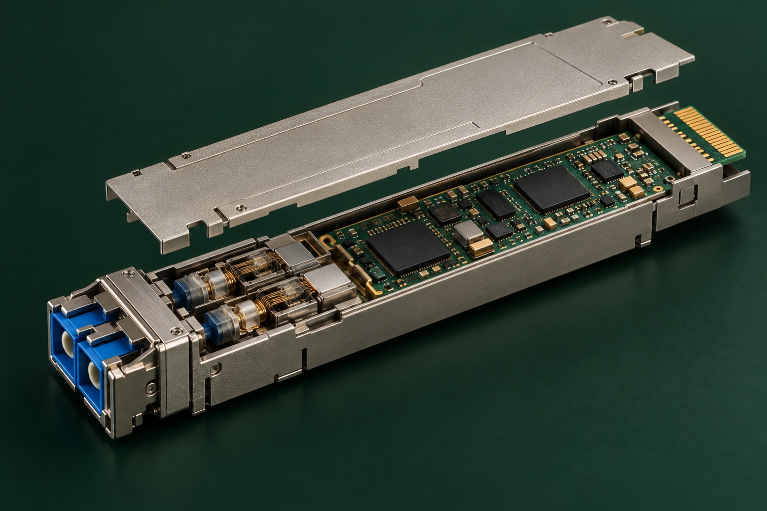
My two Fabrinet roles covered opposite ends of the same transfer. In Pathum Thani, Thailand (2013–2015), I worked on NPI and incoming technology transfers. In Santa Clara, California (2017–2019, following a 2016–2017 internship), I led optical packaging process development and developed processes for transfer to Thailand.
That factory experience shaped the development work: a process had to hold on another team’s equipment and shifts, supported by usable instructions, training, and process controls.
The scopeDeveloped die attach, wire bonding, encapsulation, and plasma-cleaning processes across multiple customer programs.
The technical depthAdhesive, eutectic, and solder-preform die attach across chip-on-board, chip-on-carrier, and chip-on-wafer. Tool ownership included improving bonder MTBA and MTBF.
The production connectionOwned and optimized print, place, reflow, and precision optical assembly steps through profiling, process windows, and qualification.
The problemPersistent delamination in lens and mirror attachment required evidence about the process variables.
My responseUsed designed experiments, temperature cycling, and detailed metrology to investigate the failure and support corrective recommendations.
The follow-throughCarried findings into 8D and material-review-board reporting so the investigation supported action.
The gapWafer assembly needed traceability and a defined response to poor yield.
My responseBuilt a VBA tracking system on Amicra die bonders. It recorded which diode went to each wafer location and reported yield and dropped-diode counts.
The controlA wafer was placed on engineering hold automatically when yield fell below 85%. This was a configured hold threshold, not a claimed achieved yield.
Explore how the work differed between receiving technology on a production floor and developing it for transfer from a lab.
As Process Engineer, refined NPI bills of material and assembly procedures, wrote manufacturing process instructions, studied product flow, and trained technicians and operators. Led two incoming fiber-rod technology transfers, from France and Singapore.
Led optical packaging process development, developing die attach, wire bonding, and optical attachment for several customer programs. Transferred the processes into mass production in Thailand. The two NPI programs covered lidar and a 400G QSFP optical transceiver; each subsequently became a $100M+ business.
The wafer tracker connected diode placement records to wafer locations, calculated yield, and triggered an engineering hold below its configured threshold. That work foreshadowed the later focus on connected manufacturing execution at Infinitum.
Establish the method, characterize variables, and qualify the process window.
Carry the method into production through instructions, training, tool readiness, and controls.
The California work included development and production transfer of two NPI programs: lidar and a 400G QSFP optical transceiver. Each subsequently became a $100M+ business. This describes the programs’ later commercial scale, not project value or revenue personally generated. The scope covered box build, SMT PCBA, and micro-optical subassemblies.
In the earlier Thailand role, improved debugging and root-cause work reduced MRB costs by $220,000. Two international fiber-rod transfers and technician/operator training complemented the process-engineering work.
Together, these roles established the foundation for my later work in lidar assembly, electric-motor manufacturing, and factory data systems.